Release time:Aug 30, 2025 Author:Teleconix Inc.
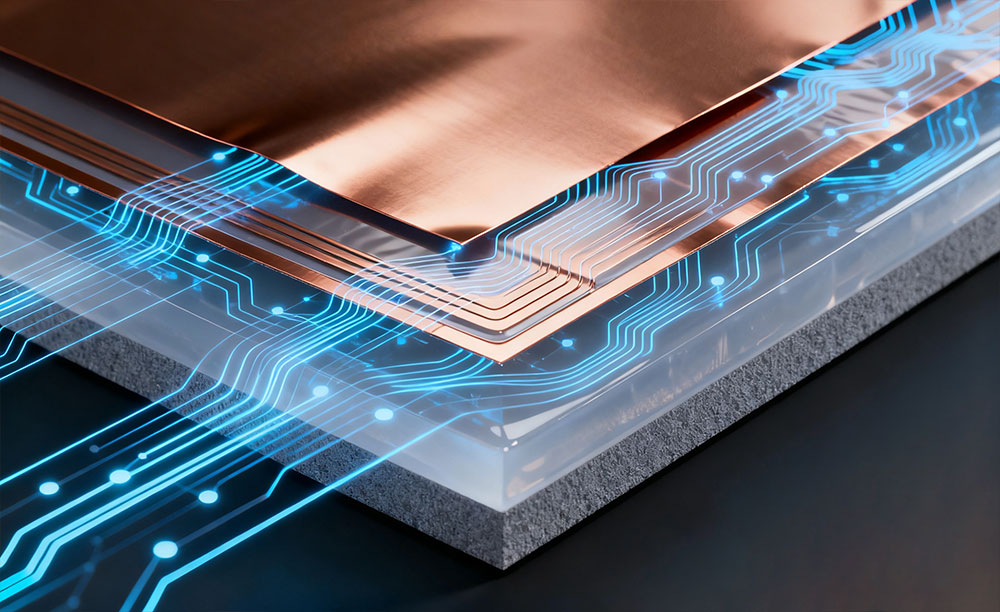
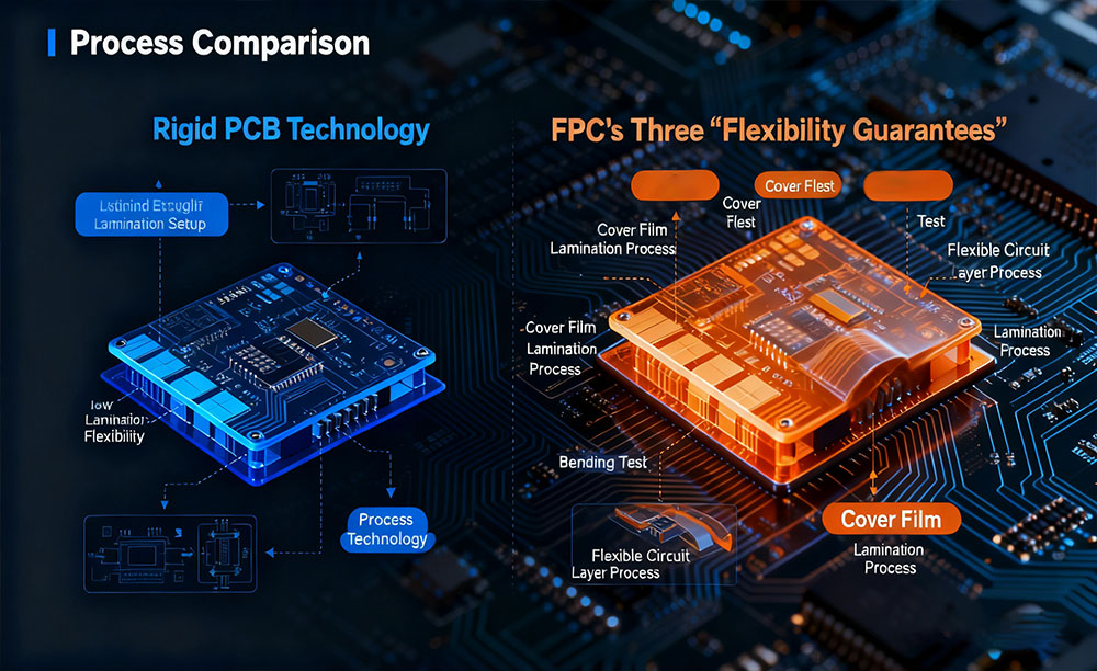
Rigid Flex PCB is a high-density interconnect product that combines the characteristics of rigid and flexible circuit boards, widely used in high-end electronic devices such as smartphones, medical equipment, aerospace instruments, etc. Its 10 layer structure achieves high integration and flexibility by alternately stacking hard and soft boards, but the production process is complex, involving precision machining and strict quality control. The following analysis will focus on structural design, process flow, production control points, and technical difficulties.
1、 Structural characteristics of 10 layer soft hard bonding board
The 10 layer soft hard composite board usually adopts a "hard soft hard" alternating stacking structure (such as 4R+2F+4R or similar combinations), where the rigid board provides mechanical support and component installation area, and the flexible board achieves bending or folding function. The key structures include:
Stacking design: The hard board and soft board are laminated with insulating bonding materials (such as PP or PI), and the soft board area needs to be covered with a polyimide (PI) protective film to avoid damage.
Conductive design: Through laser drilling and blind/buried hole technology, interlayer interconnection is achieved to ensure the integrity and reliability of signal transmission.
Partition layout: The hard board area is used for welding components, while the soft board area needs to reserve a bending radius to avoid stress concentration causing circuit breakage.
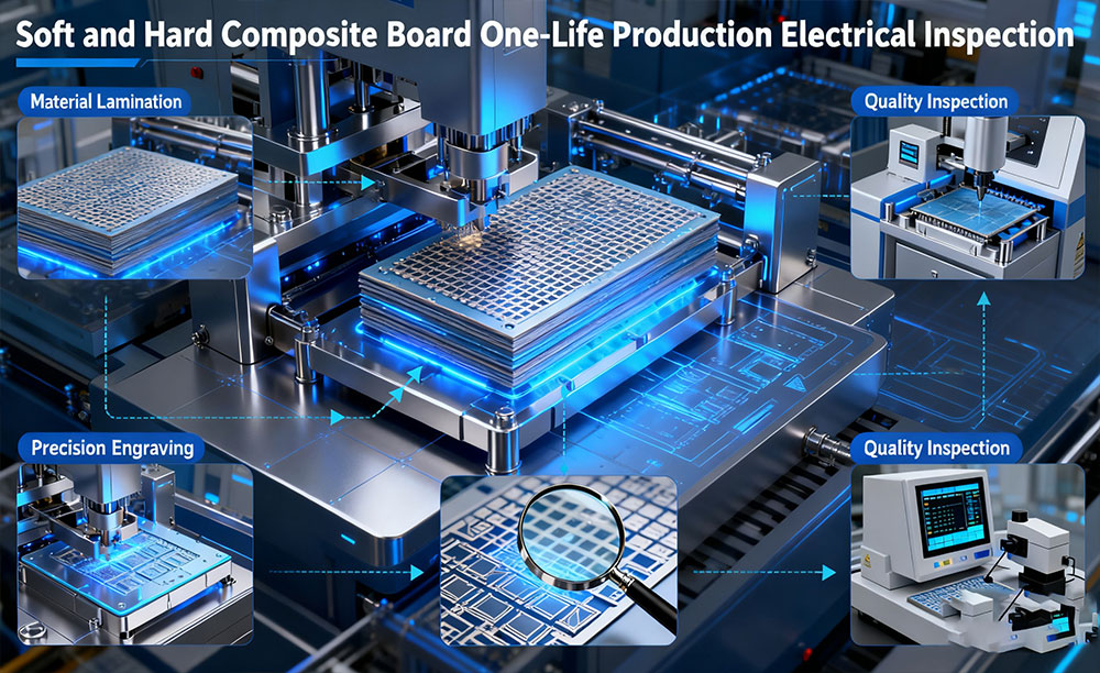
2、 Core production process flow
The production of rigid flexible composite boards involves more than 35 processes, covering key steps such as material preparation, graphic transfer, pressing, drilling, electroplating, and shape processing.
The following is the core process:
Material preparation and cutting
The hard board substrate is made of FR-4 or high-frequency materials, while the soft board is made of PI or PET base film, requiring precise control of cutting size and laminating parameters.
Hard and soft boards need to undergo plasma cleaning in advance to improve surface roughness and enhance bonding strength.
Inner layer graphic processing
Exposure and development: Line patterns are formed through dry film lamination, laser direct imaging (LDI), or traditional film exposure techniques, and excess copper layer 75 is etched and removed after development.
AOI inspection: Automatic optical inspection ensures that there are no defects such as short circuits or open circuits in the inner circuit.
Multi layer lamination and interlayer alignment
Stacking and pre pressing: Hard and soft boards are alternately stacked, and a vacuum press is used to bond them under high temperature and high pressure, controlling the flowability and overflow of PP glue.
Laser target positioning: Ensure interlayer alignment accuracy (usually ≤ 50 μ m) and avoid signal transmission problems caused by offset.
Drilling and hole metallization
Mechanical drilling and laser drilling: Mechanical drilling is used in the hard board area, while CO ₂ or UV laser drilling is used in the soft board area, with a diameter as small as 0.1mm.
Copper deposition and electroplating: Chemical copper deposition (PTH) and electroplating are used to fill the hole walls, ensuring that the resistivity of the conductive holes meets the standard.
Outer layer graphics and surface treatment
Secondary graphic transfer: The outer layer of the circuit is completed through similar exposure and etching processes, and special attention should be paid to the protection of the covering film in the soft hard bonding area.
Surface treatment: ENIG (chemical nickel gold), OSP (organic solder mask) or immersion gold process can be selected to improve welding performance and corrosion resistance.
Appearance processing and uncovering technology
Laser cutting and mechanical milling: using a combination of pre milling and laser cutting to avoid damaging the soft board area. When removing the cover, the cutting depth should be checked by slicing to ensure that the residue is ≤ 0.5mm.
Waste removal and edge treatment: By pre treating the pressed surface and milling grooves to cut through the hard board waste, the mechanical stress on the soft board is reduced.
3、 Key production control points
Electroplating and Cleaning Control
Soft boards with a thickness of ≤ 0.3mm require a specialized cleaning line for thin boards to prevent deformation; Hard boards with a thickness greater than 0.3mm and covered with a film can be polished with a stripped edge.
After electroplating, it is necessary to check whether the soft and hard joints are broken copper to avoid short circuits caused by residual chemicals.
Uncovering and shape accuracy
The parameters for uncovering need to be confirmed by slicing the first board, with a cutting depth of ≥ 15 μ m from the covering film. When manually uncovering, it is necessary to gently tear along the cutting line to avoid edge explosion or residue.
After the external processing, it is necessary to conduct a full inspection for burrs, carbonization, blackening, and other issues. The residual burrs in the soft board area are allowed to be ≤ 0.05mm.
Material and Storage Management
Sensitive materials such as shielding films need to be stored at temperatures below 5 ℃. Before use, they should be warmed up to 23 ± 3 ℃ and left to stand for 7 hours.
The covering film is not resistant to strong alkali, and it is necessary to avoid discoloration of the soft board during oil washing. Before exposure, 100% inspection of the appearance quality is required.
4、 Technical difficulties and solutions
Insufficient interlayer bonding strength
Solution: Optimize the pressing temperature (usually 180-200 ℃) and pressure, use high Tg (glass transition temperature) PP adhesive to reduce the risk of delamination.
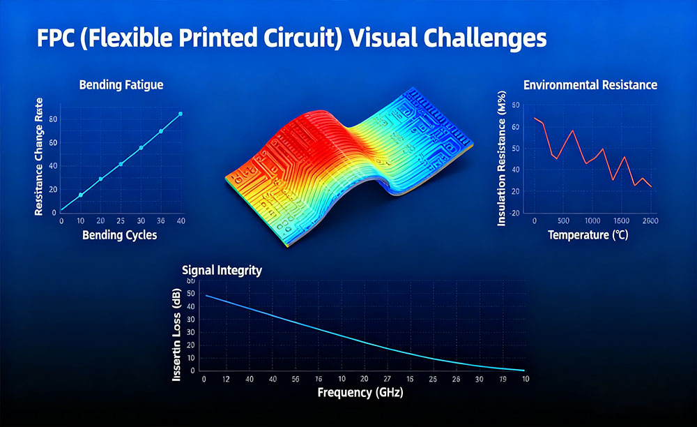
The circuit in the soft board area is prone to damage
Solution: Pre attach PI protective film in the soft board area and use laser peeling technology instead of mechanical peeling to reduce stress concentration.
Signal integrity challenge
Solution: Reduce signal interference through embedded circuit design (such as insulation bonding packaging in patented technology), and optimize transmission performance by combining impedance control technology.
The production of soft hard composite boards in PCB factories is a combination of precision manufacturing and material science, which requires high-precision control in stacking design, lamination process, and shape processing. With the increasing demand for 5G, wearable devices, and other technologies, their processes will further develop towards high-density and high reliability. Enterprises need to continuously optimize their processes (such as introducing automated AOI and laser processing technologies), while also focusing on the application of new materials (such as low loss PI films) to enhance product competitiveness.
 return

Email: rainbow@dgpoorui.com
Company Address: Building 4, Yongjianhong Industrial Park, Guangtian Road, Yanluo Sub-district, Bao'an District, Shenzhen City
Copyright © 2021 Teleconix Inc. Powered by sznbone


 CN
CN Home >